


There are sections below on ports, memory, the SDX, floppy drives and video output.
Memotech hardware components, and what they include :-
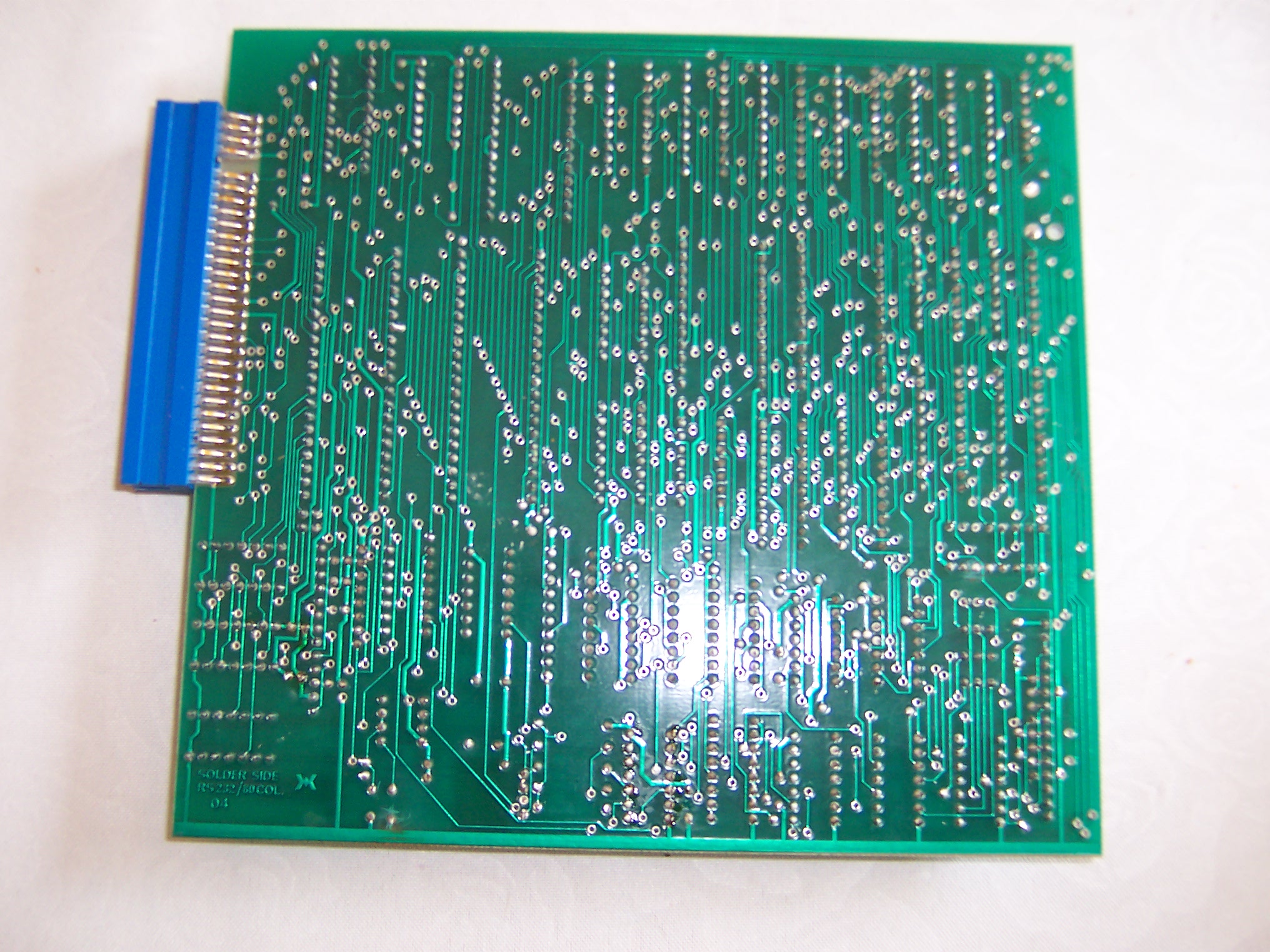
In the original design, ports below 20 hex can be provided by the Motherboard and internal/external add-ons. 20 and above were to be provided from within the FDX. This is why the FDX FDC and Sidisc ports are above 20. The RS232/interface card has logic (controlled by a PAL) to drive the data bus from the FDX to the motherboard, when port 20 or over is accessed. This PAL has to be changed if an SDX or REMEMOrizer is attached to an MTX with an RS232/interface card (and clearly the FDX cannot be connected in such a configuration).
The following table documents the original ports assigned, and what ports are known to have been used by various add-ons since then. It also gives a few indications of possible future use.
If you're thinking of designing an add-on, let me know. We can hopefully avoid collisions and keep this table up to date. Whether your add-on sits on the MTX or FDX side might influence whether you pick a port above or below 20 hex. If you're just looking for a few ports, that shouldn't be hard, but if you want lots, then depending on how many you need, maybe pick a value for A7-A0 and then further decode A15-A8?
| Motherboard | ||
|---|---|---|
| 00 | -O | IOBYTE |
| 00 | I- | Printer strobe |
| 01 | IO | VDP data |
| 02 | -O | VDP control |
| 02 | I- | VDP status |
| 03 | -O | Cassette |
| 03 | I- | Sound strobe, motherboard doesn't drive bus, REMEMOTECH and REMEMOrizer drive the value 03 |
| 04 | IO | Printer |
| 05 | -O | Keyboard drive |
| 05 | I- | Keyboard sense |
| 06 | I- | Keyboard sense |
| 06 | -O | Sound |
| 07 | IO | PIO |
| 08 | IO | CTC channel 0 |
| 09 | IO | CTC channel 1 |
| 0A | IO | CTC channel 2 |
| 0B | IO | CTC channel 3 |
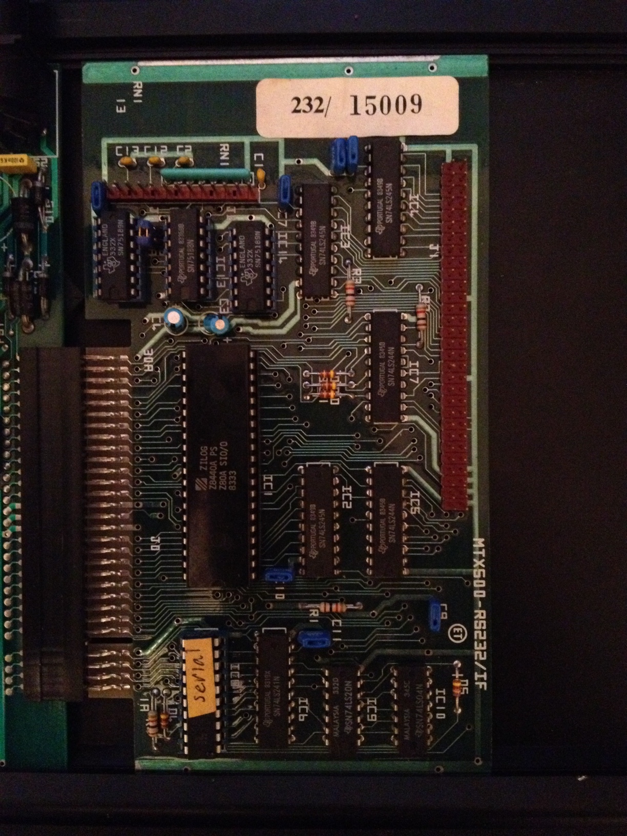
| RS232 | ||
| 0C | IO | DART |
| 0D | IO | DART |
| 0E | IO | DART |
| 0F | IO | DART |
| SDX FDC | ||
| 10 | -O | FDC command |
| 10 | I- | FDC status |
| 11 | IO | FDC track |
| 12 | IO | FDC sector |
| 13 | IO | FDC data |
| 14 | IO | Control/status port |
| Cassette controller? | ||
| 1F | -O | Cassette start/stop |
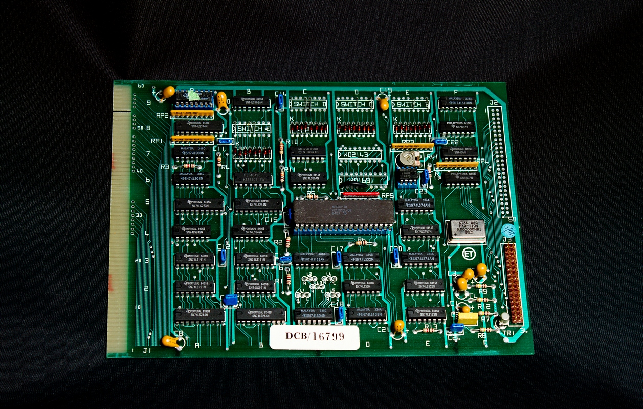
| 80 column | ||
| 30 | I- | Ring the bell (not implemented on REMEMOTECH/REMEMOrizer) |
| 30 | -O | Address low |
| 31 | -O | Address high |
| 32 | IO | Character data |
| 33 | IO | Attribute data |
| 38 | IO | CRTC register select |
| 39 | IO | CRTC register data |
| FDX FDC | ||
| 40 | -O | FDC command |
| 40 | I- | FDC status |
| 41 | IO | FDC track |
| 42 | IO | FDC sector |
| 43 | IO | FDC data |
| 44 | IO | FDC control/status port |
| 45 | IO | FDC drive change |
| 46 | IO | FDC DMA low |
| 47 | IO | FDC DMA high |
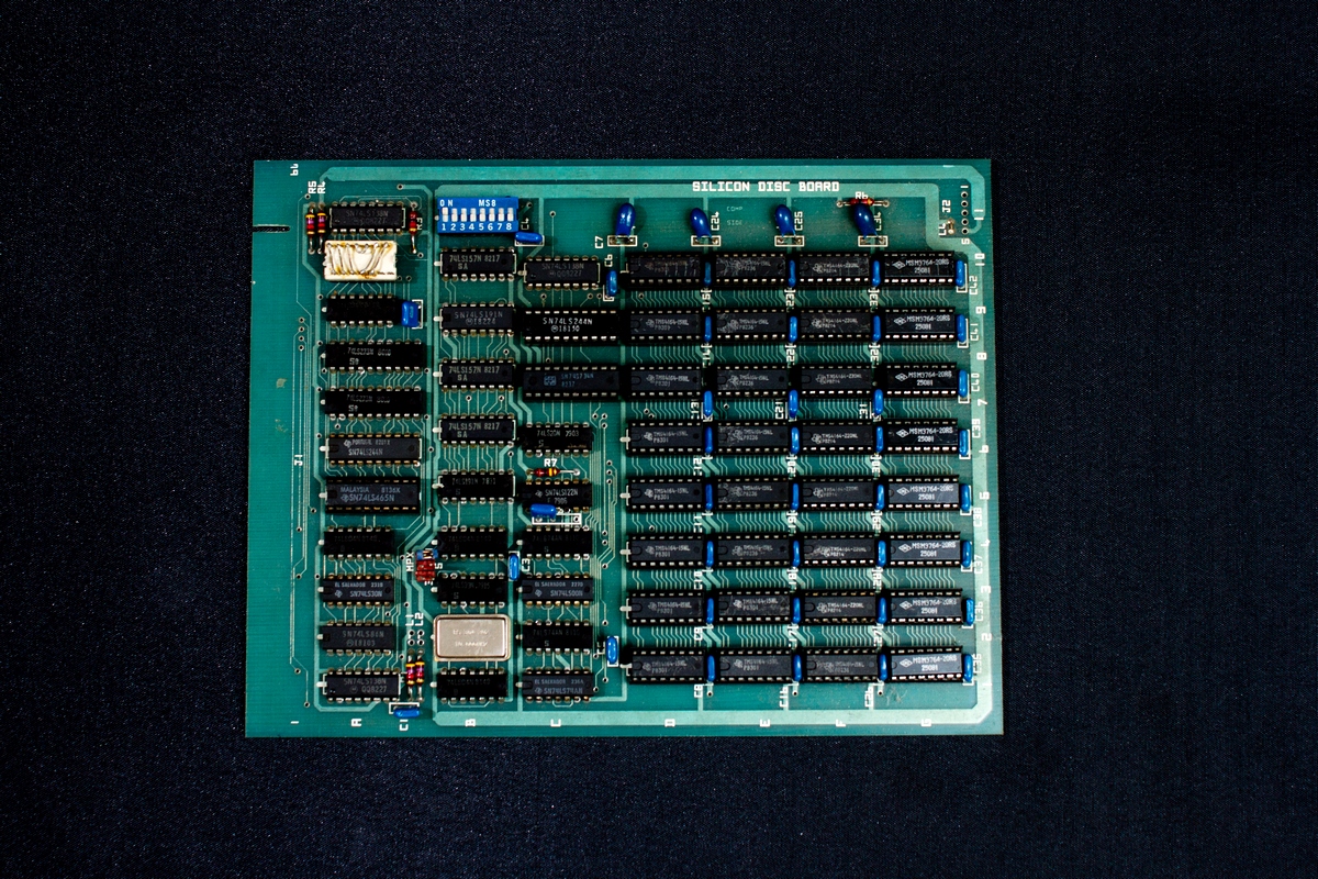
| Silicon Disc | ||
| 50 | IO | F: sector address low |
| 51 | IO | F: sector address high |
| 53 | IO | F: data |
| 54 | IO | G: sector address low |
| 55 | IO | G: sector address high |
| 57 | IO | G: data |
| 58 | IO | H: sector address low |
| 59 | IO | H: sector address high |
| 5B | IO | H: data |
| 5C | IO | I: sector address low |
| 5D | IO | I: sector address high |
| 5F | IO | I: data |
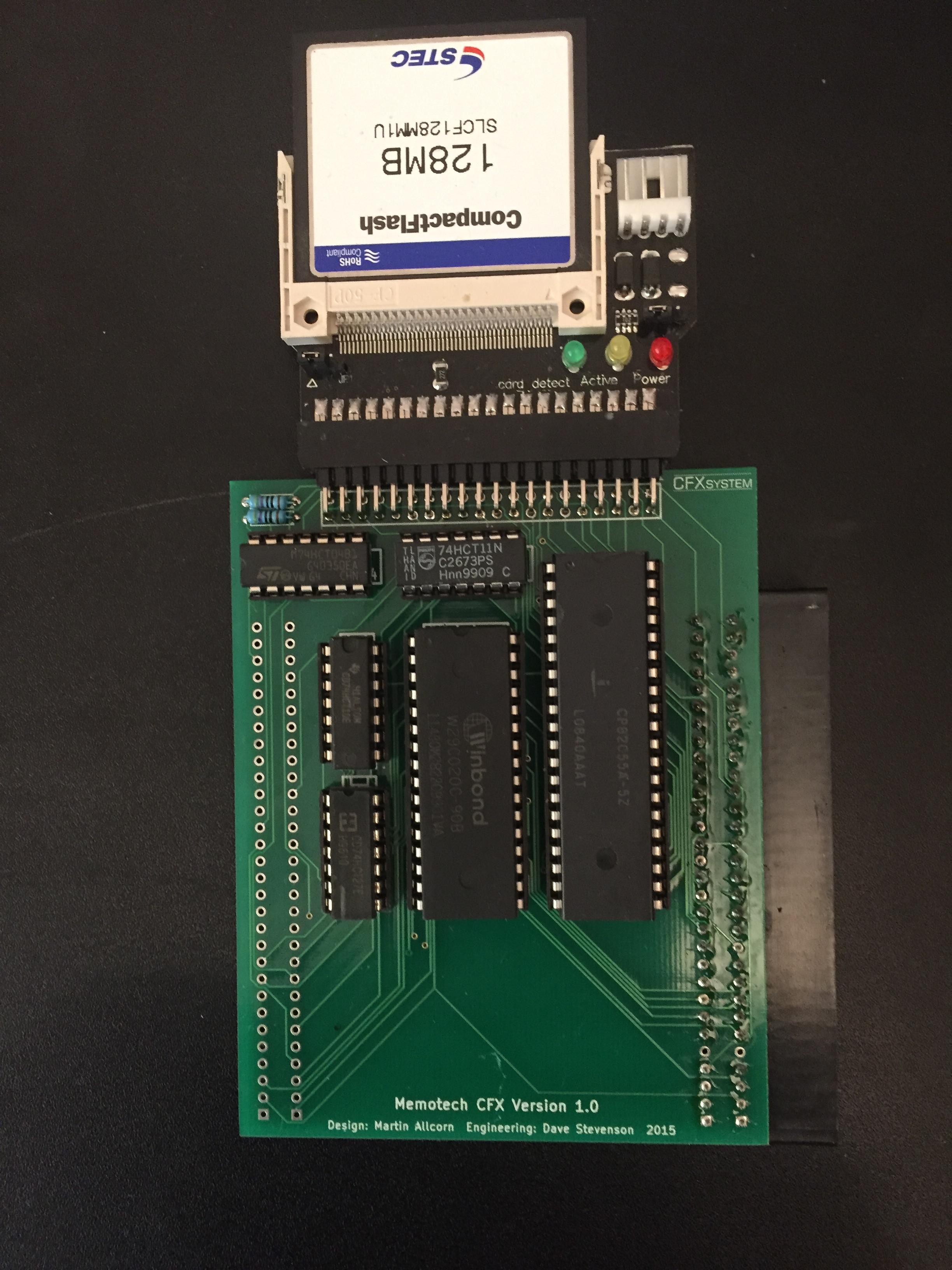
| Martins Compact Flash system (aka CFX) | ||
| 6C | IO | 82C55 PPI, PIO port A, IDE data bus, lower 8 bits |
| 6D | IO | 82C55 PPI, PIO port B, IDE data bus, upper 8 bits |
| 6E | -O | 82C55 PPI, PIO port C, IDE control lines |
| 6F | -O | 82C55 PPI, PIO control register |
| MTXplus+ | ||
| 60-63 | ?? | old MTXplus+ had 82C55 ports here, but being remapped to 6C-6F, per CFX above |
| 70 | ?? | RTC address register |
| 71 | ?? | RTC data register |
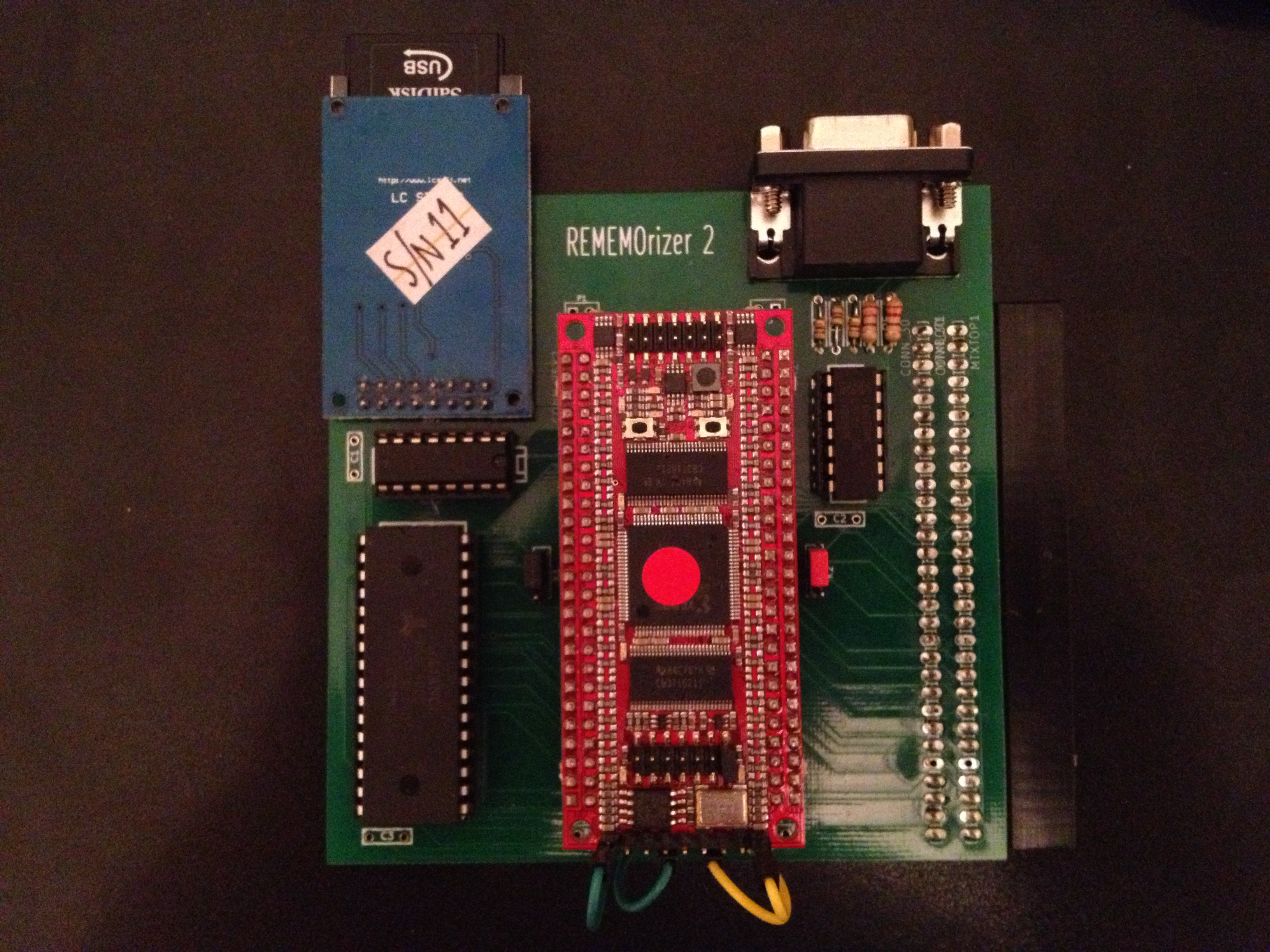
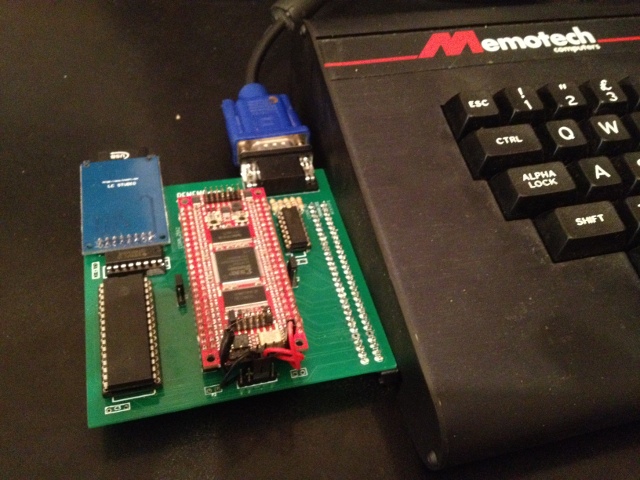
| REMEMOrizer r3 and REMEMOTECH r2 Accelerator extras | ||
| A0 | IO | Mantissa bits -24 to -31 |
| A1 | IO | Mantissa bits -16 to -23 |
| A2 | IO | Mantissa bits -8 to -15 |
| A3 | IO | Sign bit and mantissa bits -1 to -7 |
| A4 | IO | Exponent |
| A5 | -O | Command |
| A5 | I- | Result |
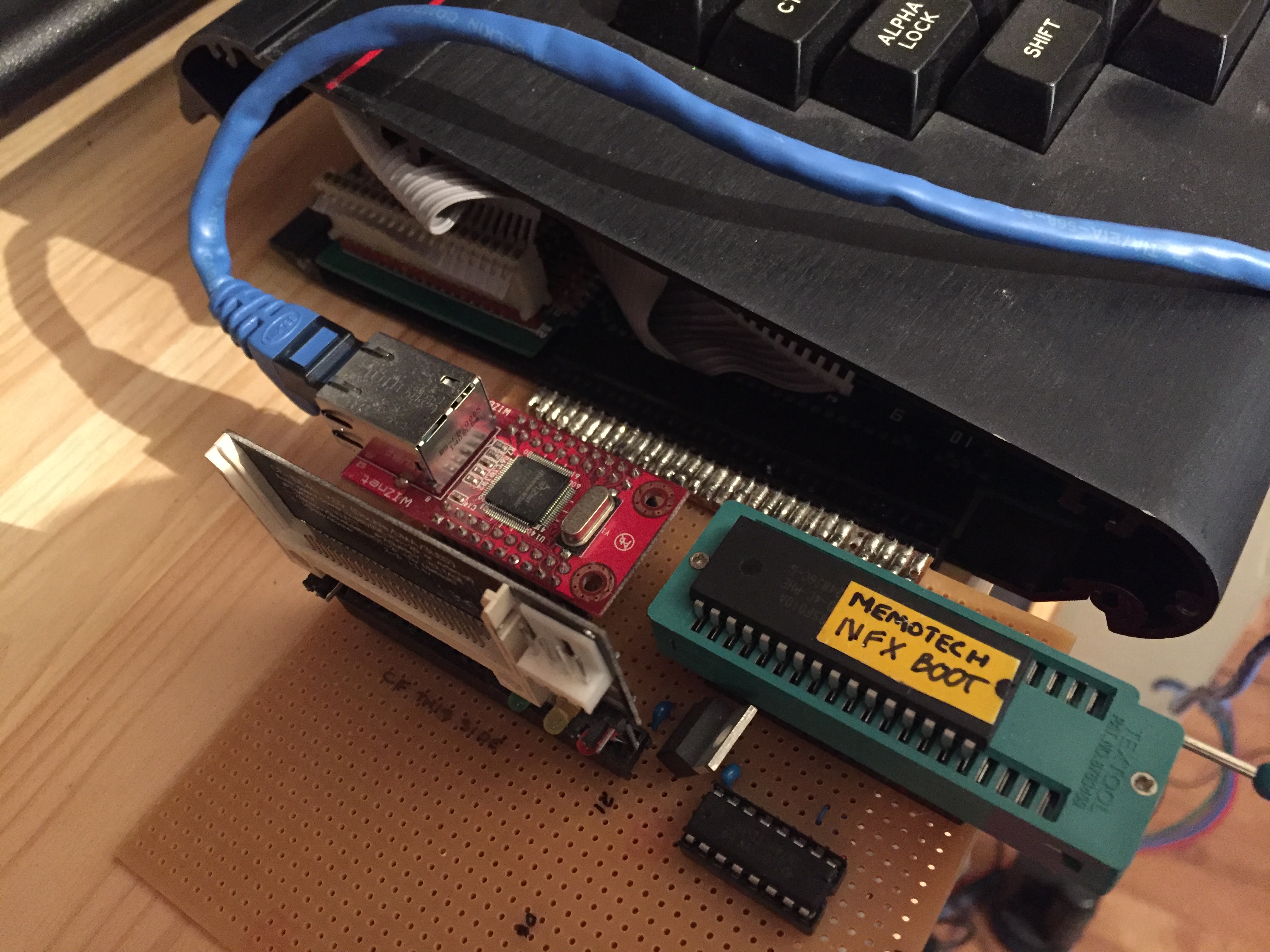
| NFX | ||
| A0 | ?O | WIZnet W5100 control |
| A1 | ?O | WIZnet W5100 address (high) |
| A2 | ?O | WIZnet W5100 address (low) |
| A3 | IO | WIZnet W5100 data |
| REMEMOrizer Speculator extras | ||
| B0 | I- | REMEMOrizer Speculator sound transition counter (low) |
| B1 | I- | REMEMOrizer Speculator sound transition counter (high) |
| B2 | I- | Video active indicator |
| B2 | -O | Row type and number select |
| B3 | I- | Run size |
| B3 | -O | Clear leftmost cell in run |
| B4 | I- | CPU address low |
| B5 | I- | CPU address high |
| B6 | I- | VDP address low |
| B7 | I- | VDP address high |
| REMEMOTECH specific bells and whistles | ||
| C0 | IO | 7 segment digits 1 and 0 |
| C1 | IO | 7 segment digits 3 and 2 |
| C2-C3 | IO | Space left for further 7 segment displays in future |
| C4 | IO | Green LEDs, LEDG7..LEDG0 |
| C5 | I- | Keys, KEY2..KEY0 (KEY3=reset) |
| C6 | IO | Space left for future features |
| C7 | I- | Extra keys, mainly numeric pad |
| C8-CF | IO | Space left for future features |
| REMEMOTECH and REMEMOrizer address mapping | ||
| D0 | IO | Page register 1 |
| D1 | IO | Page register 2 |
| D2 | IO | REMEMOrizer page register 3 |
| D3 | IO | REMEMOrizer page register 4, controls ROM 2 sub-page |
| REMEMOTECH and REMEMOrizer SD Card | ||
| D4 | IO | SD control/status |
| D5 | IO | Space left for future SD card enhancements |
| D6 | IO | SD data |
| D7 | I- | SD data, with implied send FF |
| REMEMOTECH and REMEMOrizer misc stuff | ||
| D8 | I- | Clock divider (REMEMOrizer hard codes result of 05) |
| D9 | IO | REMEMOrizer specific flags |
| DA | IO | More REMEMOrizer and REMEMOTECH specific flags |
| DB-DF | IO | Space left for future features |
| Inaki Castillo | ||
| E0-E3 | IO | Kelly Materialiser, 3 ports set vital statistics (eg: 36,24,36) and one sets desired age (eg: 21) |
| Speculator (original only) | ||
| x11xxxxx | IO | Partial address decode, covers 7E,7F,FB,FE,FF, and maybe more? |
| xxx11111 | IO | Partial address decode, covers 1F, and maybe more? |
| Speculator (original, REMEMOrizer, MEMU) | ||
| 1F | IO | Kempston Joystick |
| 7E | I- | Read emulated Spectrum border |
| 7E | -O | Write emulated Spectrum keyboard, first low bit in A15-A8 selects row |
| 7F | IO | Fuller joystick (00 written only, no button pressed) |
| FB | IO | ZX Printer (40 written only, printer not connected) |
| FE | -O | Write emulated Spectrum border |
| FE | I- | Read emulated Spectrum keyboard, first low bit in A15-A8 selects row |
| FF | -O | NMI write register |
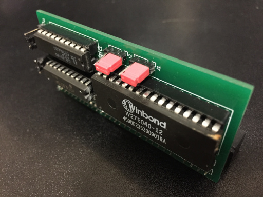
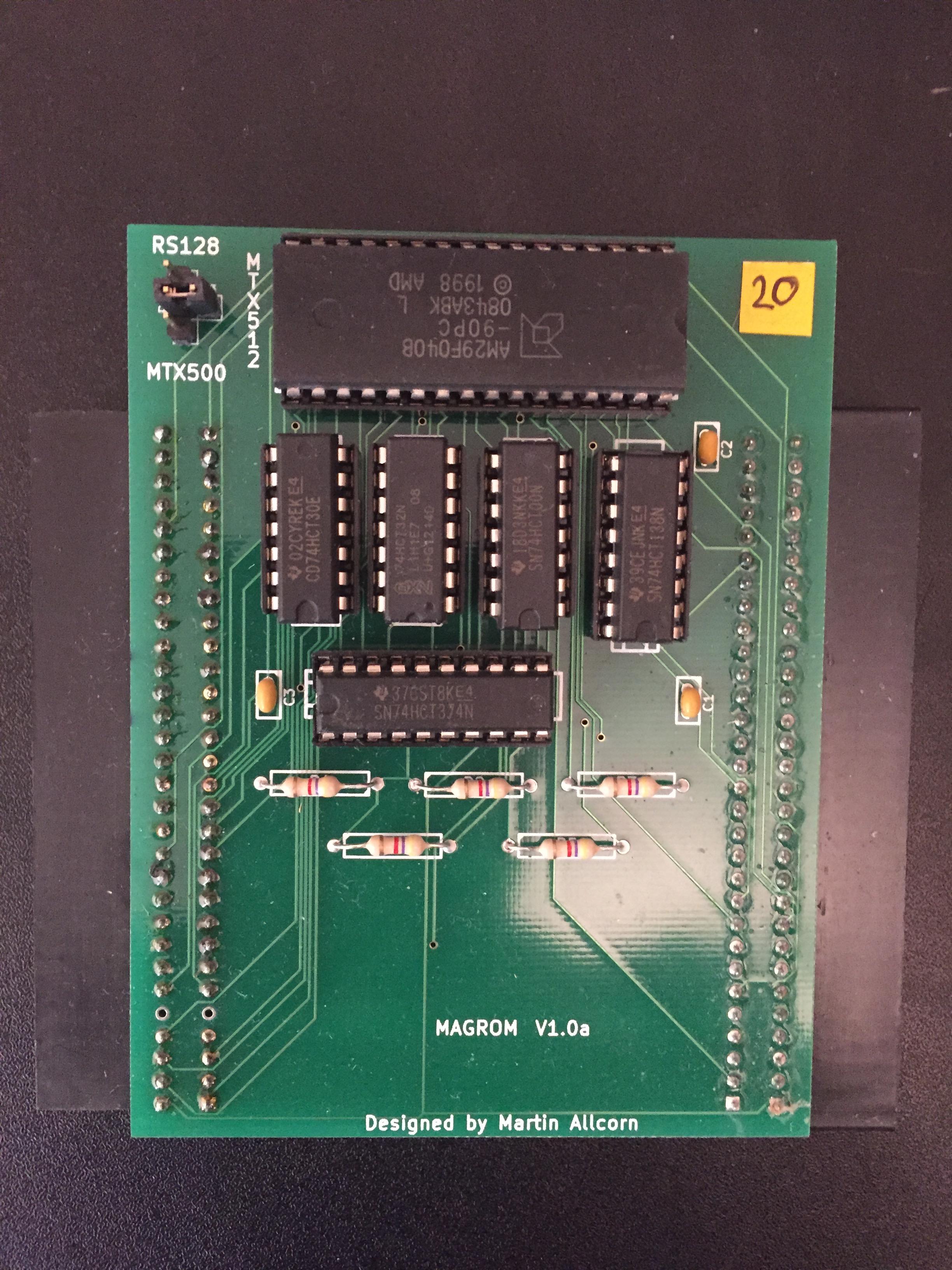
| Martins MAGROM | ||
| FB | -O | Page register for 512KB data ROM |
The memory decoder PAL, as described by the PALASM on p249 and p250 of the Phoenix MTX Operators Manual
4000-04 motherboards have a 16KB ROM and an 8KB ROM. 4000-05 motherboards have 3 x 8KB ROMs.
The PALASM for a system with 16KB + 8KB ROM should include this :-
/CEA  = /RELCPMH                   * /A15 * /A14 * /A13 * /MREQL * /RDL
      + /RELCPMH * /R2 * /R1 * /R0 * /A15 * /A14 *  A13 * /MREQL * /RDL
/CE64 = /RELCPMH * /R2 * /R1 *  R0 * /A15 * /A14 *  A13 * /MREQL * /RDL
      + /RELCPMH *  R2 *  R1 *  R0 * /A15 * /A14 *  A13 * /MREQL * /RDL
CEA recognises the fixed ROM and ROM page 0.
CE64 recognises ROM pages 1 and 7. CE64 is further decoded outside the PAL.
The PALASM for a system with 3 x 8KB ROM should include this :-
/CEA  = /RELCPMH                   * /A15 * /A14 * /A13 * /MREQL * /RDL
/CE64 = /RELCPMH * /R2 * /R1       * /A15 * /A14 *  A13 * /MREQL * /RDL
      + /RELCPMH *  R2 *  R1 *  R0 * /A15 * /A14 *  A13 * /MREQL * /RDL
CEA recognises the fixed ROM.
CE64 recognises ROM pages 0, 1 or 7. CE64 is further decoded outside the PAL to distinguish between ROM pages 0 and 1, and ROM page 7, known as the "games ROM".
Claus Bækkel has a Danish MTX which a little 1KB ROM piggy-backed on to one of the other ROMs. This ROM is enabled by ROM 7, and contains code which redefines certain characters in the pattern generator table, so that they are now certain danish characters. In addition, it intercepts the keyboard routine and changes the behavior of the CTRL key with these characters.
There is a hard-wired link just above the PAL at position A6, known as LK7, and this signal referred to in the PALASM as I2H4L. In the MTX512 I believe this would be wired to 4, ie: low. On my MTX500 it is wired to 2, ie: high. I think this link is probably a hangover from originally attempting to have one PAL which would handle MTX500 (2x16KB) and MTX512 (4x16KB). Although the original PALASM references I2H4L, I ignore it here.
An MTX500 has 8 x 4132 DRAM chips (or similar, eg: my MTX500 uses M3732L-20RS). The 6-pin LK6 link block at position B7 on the motherboard controls which address lines are passed to the DRAMs and how, and certain combinations allow an MTX500 motherboard to use half-working 4164 chips instead.
The PALASM for a system with 32KB DRAM should include this :-
/NA15 =                                    /A15
/RAM  =                                     A15 *  A14 * /MREQL
      +            /P3 * /P2 * /P1 * /P0 *  A15 * /A14 * /MREQL
There are bugs in the MTX500 PALASM. DRAM appears in places where it shouldn't. Where DRAM inappropriately appears depends on the number of ROMs. Before adding additional memory, memory decoder PALs programmed differently to the Phoenix Manual are needed.
An MTX512 has 8 x 4164 DRAM chips (or similar). Some systems labelled MTX512 are actually an MTX500 (ie: 32KB on the motherboard) with a memory expansion card with an additional 32KB of memory.
The PALASM for a system with 64KB DRAM should include this :-
/NA15 =                                    /A15
      + /RELCPMH * /P3 * /P2 * /P1 *  P0 *  A15 * /A14
/RAM  =                                     A15 *  A14 * /MREQL
      +  RELCPMH * /P3 * /P2 * /P1 * /P0               * /MREQL
      + /RELCPMH * /P3 * /P2 * /P1 * /P0 * /A15 *  A14 * /MREQL
      + /RELCPMH * /P3 * /P2 * /P1       *  A15 * /A14 * /MREQL
The NA15 equation remaps accesses in RELCPMH=0 mode, to RAM Page 1, Z80 addresses 0x8000-0xbfff, to DRAM addresses 0x0000-0x3fff. Put another way, this is how the δ page moves between RELCPMH modes.
The MTX512 S2 is basically just a yellow wire modification of the original MTX motherboard, allowing the use of larger DRAMs. This upgrade was not (and can not be) 100% compatible with previous MTXs - the δ memory page doesn't move correcly between RELCPMH modes.
An MTX512 S2 has 8 x 4256 DRAM chips. At first glance, it might appear this would have 256KB of RAM. However, from BASIC (ie: in RELCPMH=0) mode, there is only 64KB visible, and from CP/M (RELCPMH=1) mode, 208KB of RAM is visible.
The /CAS signal into the DRAMs is altered. The A7 input to the DRAMs is normally multiplexed from A14 and NA15 (where N15 is the new A15 computed by the address decoder PAL). However, this is now simply multiplexed from A14 and A15.
What was previously the NA15 output of the PAL now effectively provides A16 and A17 to the DRAMs. Which to provide depends on the RAS/CAS logic, so the the I2H4L input to the PAL is repurposed and feeds the MPX signal from the RAS/CAS logic.
The PALASM for a system with 256KB DRAM should include this :-
/MA8  = P0 * MPX
      +                                     A15 *  A14
/RAM  =                                     A15 *  A14 * /MREQL
      +  RELCPMH * /P3 * /P2                           * /MREQL
      + /RELCPMH * /P3 * /P2 * /P1 * /P0 * /A15 *  A14 * /MREQL
      + /RELCPMH * /P3 * /P2 * /P1       *  A15 * /A14 * /MREQL
MPX is the repurposed I2H4L pin, and MA8 is the repurposed NA15 pin.
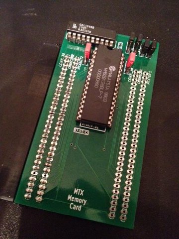
Upgrading MTX500 to MTX512
I now recommend the use of an MTX Memory Card with an appropriate GAL and SRAM memory chip in it. With this approach there is no danger of damaging the MTX motherboard whilst desoldering the DRAM chips (as I did to mine). Alternatively, if you're confident of your skill with a soldering iron and desoldering pump, read on...
This datasheet has a picture of PAL pin-outs, including the PAL14L4. However, you'll find it hard to find software you can easily install and use. I've tried PALASM 2.3d, PALASM 4.15, under DOSEmu, DOSBox, and FreeDOS on real hardware. You might also find it hard to find a PAL programmer.
GAL16V8s can be programmed with the same equations as PAL14L4s (and many other 20 pin PAL types), and are pin compatible.
I've found it best to use the Opal junior 2.1 tools to compile the equations to a JEDEC file, and TopWin Ver 6.22 and a TOP853 programmer to program a GAL16V8 instead.
Recommended procedure (not successfully performed as yet) :-
PRINT PEEK(64122) should now return 1, rather than 0.
Note, the above procedure does not suggest breaking and remaking the I2H4L link, close to the PAL chip at A6 on the motherboard. Instead, I suggest you use equations for 64KB RAM that simply do not reference the I2H4L input. One less thing to mess up soldering.
Here are the equations to use with GAL16V8s :-
| 0KB RAM | 32KB RAM | 64KB RAM | 64KB/208KB RAM | |
|---|---|---|---|---|
| 2 ROMs | 2_0 .eqn .jed | 2_32 .eqn .jed | 2_64 .eqn .jed | 2_208 .eqn .jed |
| 3 ROMs | 3_0 .eqn .jed | 3_32 .eqn .jed | 3_64 .eqn .jed | N/A |
The 0KB RAM files are for use if you have screwed-up a motherboard DRAM
upgrade, of if the DRAMs on the motherboard are faulty.
You'd then need a memory card of some kind to operate the MTX.
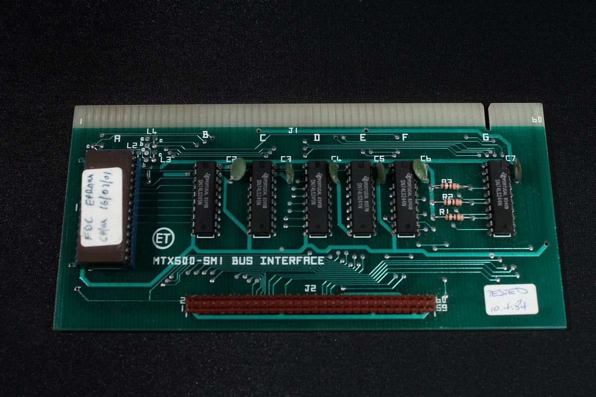
SDX hardware investigation
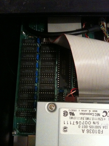
My one-off special SDX has he newer wider circuit board, with the 512KB of DRAM and 16KB ROM (slots 4 and 5). It's connected to a single 3.5" NEC FD1036A floppy drive.
My older SDX has the older thinner circuit board, without any extra DRAM. Originally it had a single 8KB ROM (slot 3) but I upgraded it to have 16KB ROM (slots 4 and 5). The CP/M ROM in slot 4 supports B:07,C:07 and the SDX ROM in slot 5 supports B:07. It is now connected to a Epson SD800 dual 3.5" and 5.25" combo drive. I have it wired so that B: is 3.5" and C: is 5.25", although with different wiring or jumper settings, it could be the other way around. I had to configure the 5.25" drive so that it runs at 300rpm, which is consistent with the information for "5.25 inch drives, 720K DD, 80 track" in Herbs technical information.
The SDX FDC circuit diagram covers the older SDX, but the later one is likely to be very similar, except with extra memory.
Both styles of controller support Shugart floppy disk drives, and these differ slightly from the more modern drives used in IBM PCs, refer to these pinout tables.
To connect a PC controller to Shugart drives, a forum post includes this diagram :-
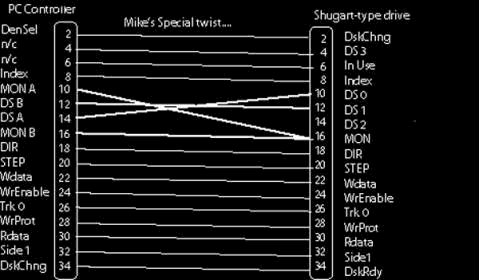
To connect a SDX FDC to a modern drive, we need to do the reverse.
The SDX controller pulls "disk change detect" aka pin 2 low. On modern 5.25" drives this is "density select", so this means we only support double-density on a single-density and double-density capable drive. Presumably a single-density only drive ignores this signal, so in that case we'd only be supporting single-density. On modern 3.5" drives the drive uses the HD hole on the diskette to spot whether it is double-density or high-density (so ensure this is taped over on the floppy diskette), so again, we only support double-density. I don't think we ever saw any single-density 3.5" floppy drives, or any diskettes formatted as single-density. There never was any support for high-density in any Memotech product. The double-density type codes are 02, 03, 06 and 07.
I am not sure whether the difference between "disk change" and "disk ready" on pin 34 is ordinarily a problem or not, although the SDX FDC circuit diagram doesn't appear to use this signal.
Aside: the SDX FDC circuit diagram seems to show DRIVE SELECT 3 being mapped to pin 6 rather than the pin 4 per Shugart specification. Probably a problem with the diagram, but it wouldn't matter if this was really the case - modern drives don't use either pin 4 or 6.
On my one-off special SDX, when booting from B:, I see pin 10 go low. So the FD1036A is configured to be "drive 0". When trying to boot from C:, I don't see any pin go low. So I don't see how I can connect two drives at once.
My older SDX is able to drive two drives, which conveniently I provide in the form of an Epson SD800.
Beware: Most literature I can find numbers the pins as shown on this page.
However, the SDX FDC circuit diagram and the SDX FDC circuit board number
the pins in reverse.
So pin N becomes pin 35-N.
This means the red-edging on the Memotech supplied ribbon cable is pin 1
according to SDX convention, but actually pin 34 according to Shugart and
modern drive convention.
This also means that a conventional PC style floppy cable (with its notch
to prevent incorrect connection) fouls the SDX FDC PCB.
Floppy advice
Mike Rudkin offers the following advice when trying to get the original Qume 142 floppy drives working again...
I find that after some years, especially if not used, the shiny metal head-guide rail becomes dry and maybe even covered in fluff/dust ... especially at each end. (They tend not to become worn as such, as the steel is high quality and very dense on these early 80's drives).
If you can very gently get the head guide rail clean and fluff free (Tweezers then a cotton bud soaked in (tape head cleaning) Isopropyl alcohol should work wonders), then leave it for 10 minutes... before you apply an extremely small amount of spindle oil (watchmakers or sewing machine oil is great).
Put a little tiny drop of oil on the rail, then move the head carefully up and down the rail a few times. After doing this, if you can see any residual oil at all... then you need to wipe it off. Basically any residual trace amounts of oil under the head runner will suffice for at least another 10 years!
Then before you re-install the drive, make sure that any moving parts/springs etc don't have any fluff or dust on them.
Your drive will now be able to self adjust the head position accurately... as it did when it was new.
The only drawback "might" be that if you have any disks that were useable/formatted whilst the disk was going out of alignment, you might find that after this procedure, they are unreadable. This can be got around by fixing one drive, then copying all your disks to that drive from the other "dirty" drive BEFORE it is cleaned/fixed in the same way.
It is always good practice to also clean the edge connector of the
drives before re-fitting... use either an eraser or Isopropyl alcohol.
Video Output
The MTX VDP output goes through a TV standard specific (PAL, NTSC, ...) video daughter board, through a UHF modulator, and then on to your TV. Analogue TVs are getting harder to find and are big bulky things. Also, as the MTX warms up, so the frequency of the signal drifts, requiring continual retuning.
Instead, I remove the daughter card, and attach this cable :-
The block at the bottom is a 5-pin female header block, and on the right we have composite plugs and a 3.5mm socket.
I then convert the composite signal to VGA using a Gonbes 8200 :-
The picture quality isn't brilliant, but its better than my TV. It can show junk around the main picture area, and overall the picture is bluer than it should be, with no obvious way to tune. This may require resistors in the cable, but I've not worked out any of this as yet.
I also connect the 3.5mm socket through a 3.5" male-to-male cable and into the VGA monitor, so I get sound too.
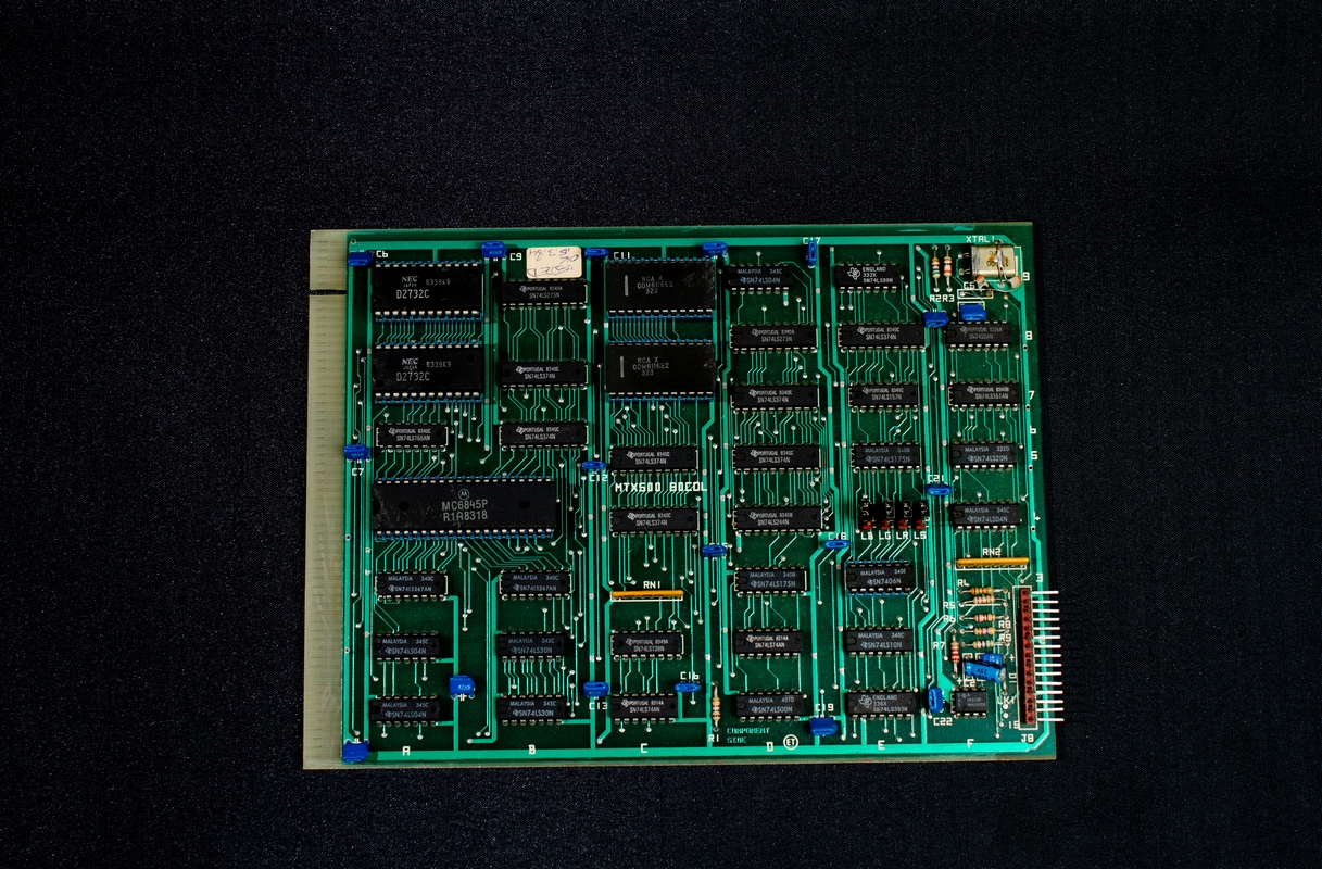
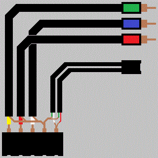
If you have a FDX or an SDX you may have the 80 column card. This outputs a colour signal out of a 9-pin female connector. The problem is that this signal is for old monitors, and can't be fed to a modern VGA monitor. This too can be converted to VGA using a Gonbes 8200, using this cable :-
The diagram shows the back of the 9-pin plug, and the 8-pin cable supplied with the Gonbes 8200. The colour coding reflects the colours on the cable. Red, green and blue are obvious. Black is ground and grey is sync.
Some adjustment of the presets on the Gonbes are required to get the colour bright enough.
The Gonbes 8200, composite cable (cut in half), 3.5mm male-to-female cable (cut in half), 5-pin female header, 5V 2A PSU, and 9-pin Dsub male plug can all easily be found on eBay.