The idea behind the hardware design was to minimise the chip count, and soldering it all together myself (badly). Instead use :-
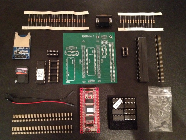
Here are the parts :-
Use a GODIL that has :-
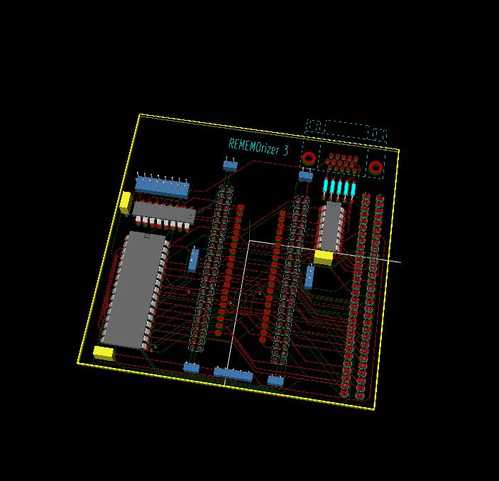
Circuit diagram created in KiCad, which when placed and routed looks like this.
I've also added the all.tar.gz library of extra converted
parts from
http://library.oshec.org/
to my installation of KiCad.
The board design has provision for a 40-pin DIL socket, thus supporting GODILs with 40 pin DIL pins. When this kind of GODIL is used, fly-leads are needed from nearby headers to the headers on the GODIL, in order that the signals to the SRAM can be made available. The board design also has provision for 50-pin headers, thus supporting GODILs with 50-pin female IDCs. A benefit of supporting 50-pin IDC GODILs is that the connections to the SRAM socket are now taken care of, with no need for the ugly fly-leads.
The VGA related output of the GODIL goes through a 74HCT04 hex inverter so as to clean up the voltages and hide the charge and discarge effects from the FET based bus-switches on the GODIL. This means I must generate the negation of the VGA signals, so that the hex inverter will re-negate them, producing the right output. This massively improves output quality - no smear or fading, although with a little shimmer.
The reset circuit on the MTX uses a kind of pull-up resistor, and so does the GODIL on every input. The net effect is that if you connect them together and press the reset keys, the voltage doesn't drop enough, so neither the MTX nor the FPGA resets. So /RESET on the motherboard is passed through the inverter so as to produce a RESET signal that is either a strong high or a strong low. I had to deglitch the RESET signal to stop spurious resets of logic in REMEMOrizer.
Dave observed SD Card problems on his REMEMOrizer(s) on his MTX000. Investigation pointed to noise on the PHI (4MHz CPU clock) signal, and so the REMEMOrizer r2 design deglitches the PHI signal and uses the cleaned up signal to drive the SD Card hardware.
The SD Card related output of the GODIL goes though a 74HC4050 hex high to low level changer, so as to ensure the SD Card is fed with signals at the 3.3V level. This significantly improves reliability.
I originally implemented the various ROM images within the FPGA as asynchronous memory. As I added more of these, I found the Synthesis times (the first major compilation step) took longer and longer, until eventually I gave up waiting for it to finish. You're not really supposed to be doing asynchronous memory in an FPGA, so I looked at the Z80 timing diagrams, and realised I should be able to use synchronous memory. However, when I clocked the memory with the 4MHz Z80 clock, it didn't work. I need to clock it with the 49MHz GODIL clock to make it work. I suspect the bus signals aren't actually as clean as the Z80 timing diagrams would suggest.
As I now run on Fedora 27 x86_64, I need to run Xilinx ISE like this :-
$ . /opt/Xilinx/14.7/ISE_DS/settings64.sh
$ cd ~/mtx/rememorizer/ise
$ LD_PRELOAD=$XILINX/lib/lin64/libstdc++.so:$XILINX/lib/lin64/libTw.so ise
I originally put the preloads to prevent XST crashing with a "double free" bug, but I'm not sure if I still need them.
I prefer to use xc3sprog instead of iMPACT. I can program non-persistently over JTAG using :-
$ xc3sprog -c xpc -v rememorizer.bit
However, the Xilinx drivers package for their Platform cable doesn't work on recent Linux, so I had to patch them, per this post on the Xilinx forums.
xc3sprog doesn't seem to have
bscan_spi/xc3s500e*.bit to get
the FPGA to act as a bridge to programming the SPI.
So I've hacked one of the Verilog samples which is for a board with a
XC3S500E chip, adjusted for the pinouts of the GODIL, and made my own.
I can therefore do this :-
$ xc3sprog -c xpc -v -Ixc3s500e_godil.bit rememorizer.bit
Naturally I have sent this SPI loader to the company responsible
for GODILs and to the mailing list for xc3sprog,
and I include a copy in the REMEMOrizer package.